10+ 8255 block diagram
8255 Connection to LCD 1. Describe the Block diagram of 8255.
8255 Programming
Data busD 0 -D 7.
. 8255 PPI contains 24 programmable IO pins arranged as 2 8-bit ports 2 4-bit ports. These are eight port A lines that acts as either latched output or buffered input lines. Programmable Peripheral Interface - Introduction2.
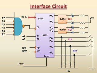
Programmable Peripheral Interface Block Diagram. It consists of data bus buffer control logic and Group A and Group B controls. The LCDs RW pin is connected to.
142 shows the internal 8255 block diagram of 8255 Pin Diagram Microprocessor. The signal description of 8255 are briefly presented as follows. In this video the following topics are covered1.
8255 PPI contains 3 ports and they are arranged in two groups of 12 pins. Pins and Signals Block Diagram3. The LCDs RS pin is connected to PB0 of Port B of the 8255.
These are 8 -bit bi-directional buses connected to 8085 data bus for transferring data. 2 Pin Diagram of 8255. Solve only Part B a Draw a block diagram of a microprocessor based system interfaced with 8255 8254 8259 8237and RAMAlso show clock generator buffers transceivers and address.
The LCDs data pins are connected to Port A of the 8255.
8255 Programming

Motorola 6800 Wikiwand
2

2019 2 3l Ecoboost Water Pump Housing Part Number Ford Mustang Ecoboost Forum
8255 Programming
What Is What If Analysis In Microsoft Excel Quora

Motorola 6800 Wikiwand

Qfp64 0 5 Rev2 Adapter
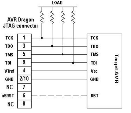
Keyboard Interfacing With Avr Javatpoint
2

8255 Programming
8255 Programming

8255 Programming
2
Atmega32 Pin Diagram Javatpoint
2
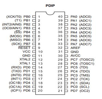
Atmega32 Pin Diagram Javatpoint